
Quantum dots reveal plasmons moving along metal surfaces
Osaka Metropolitan University researchers used fluorescent quantum dots to image hidden plasmon waves with a standard optical microscope.
By Tom Brennan · Health & Medicine Correspondent
3 min read
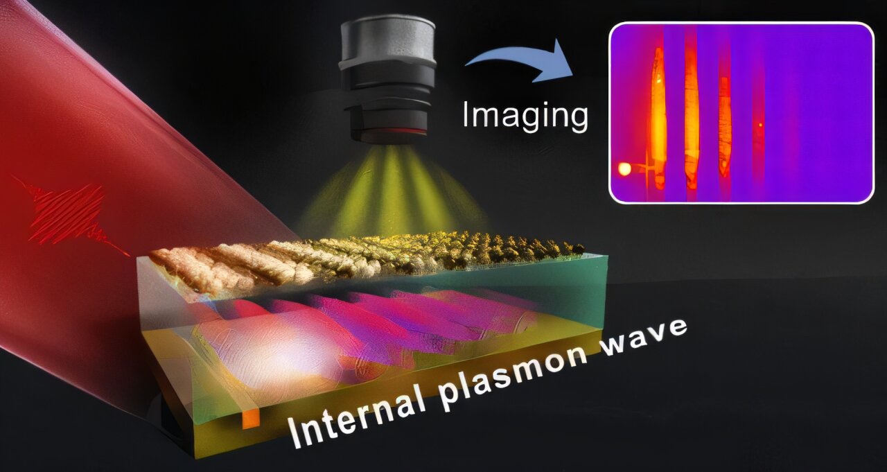
Researchers at Osaka Metropolitan University say quantum dots reveal plasmons that are usually hidden from direct view, offering a new way to study light waves that move along metal surfaces. The method, reported in Nano Letters, could help engineers examine plasmonic devices under more realistic conditions.
The work focuses on surface plasmon polaritons, or SPPs. These are electromagnetic waves that travel along the boundary where a metal meets a dielectric material such as air or glass, rather than spreading through open space like ordinary light.
Because SPPs remain tightly confined to that interface, researchers view them as useful for nanoscale optical circuits, sensitive sensors and quantum devices. Masahiro Shibuta, an associate professor at Osaka Metropolitan University’s Graduate School of Engineering and lead author of the study, said direct imaging of their movement has been difficult, especially in complex structures or at buried interfaces.
How do quantum dots reveal plasmons?
The Osaka Metropolitan University team coated a metal surface with an ultrathin film of fluorescent quantum dots, which are semiconducting nanoparticles that emit light. According to the researchers, the dots worked as sensitizers: they absorbed energy from the plasmon waves and converted that interaction into visible optical signals.
In the experiment, a near-infrared femtosecond laser produced SPPs on the coated surface. The waves then excited the quantum dots, which emitted upconversion fluorescence, a process in which multiple lower-energy photons are turned into one higher-energy photon.
That fluorescence produced alternating bright and dark fringe patterns. The researchers said those patterns traced the plasmon waves in space and time, allowing them to be recorded with a conventional optical microscope under ordinary laboratory conditions.
Shibuta said the technique makes it possible to observe SPPs in ambient conditions, including at interfaces hidden beneath other material, and to evaluate their wave properties from optical images.
Why buried interfaces matter
Previous approaches for SPP imaging have often depended on exposed metal surfaces, according to Osaka Metropolitan University. The new method was shown at interfaces covered by relatively thick dielectric films, which makes it more relevant to practical plasmonic devices that are built from layered materials.
The researchers also used the fluorescence patterns and time-resolved images for measurement, not only visualization. They reported that the images showed how dielectric films change SPP propagation, including wave velocity and dispersion, and that the experimental results closely matched theoretical predictions.
The team further found that plasmonic behavior changed with the number of quantum-dot layers on the surface. From that response, the researchers determined the dielectric constant of the photofunctional layers, showing that the approach can characterize both plasmon waves and the optical properties of nanomaterials used in plasmonic devices.
The study was published as “Visualization of Internal Plasmonic Wave Photosensitized by Quantum Dots” by Kazuki Kamada and colleagues in Nano Letters. Osaka Metropolitan University said the group next plans to apply the method to more complex plasmonic and photonic systems.
Shibuta said the longer-term aim is to create a broadly usable platform for visualizing and controlling plasmonic phenomena, with potential uses in nanophotonic and optoelectronic device development and in studies of light-matter interactions at the nanoscale.
This story draws on original reporting from Phys.org.