
Photonic circuits inverse design yields smaller foundry-ready chip parts
Max Planck and Harvard researchers report silicon nitride photonic components up to 500 times smaller than conventional designs.
By Tom Brennan · Health & Medicine Correspondent
3 min read
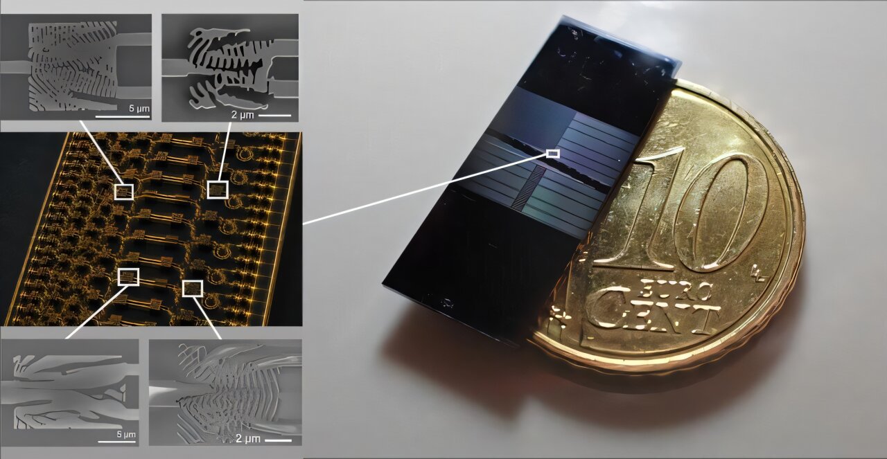
Researchers at the Max Planck Institute for the Science of Light and Harvard University have used photonic circuits inverse design to make three working chip components far smaller than conventional versions. The work matters because compact, manufacturable photonic parts could help pack more light-based functions into chips used for telecom, AI data centers, measurement systems and quantum technologies.
The team reported the results in Nature Communications. According to the Max Planck Society, the devices were designed, fabricated and tested in thick silicon nitride, a low-loss material platform used in high-performance integrated photonics.
What is inverse design for photonic circuits?
Inverse design is a computer-based method in which researchers define the optical behavior they want, then let an algorithm search for a nanostructure that can produce it. Instead of starting from a familiar component shape and tuning it by hand, the software may arrive at irregular patterns of holes and ridges that guide light in ways a human designer might not draw.
Photonic microchips move and process information using light traveling through tiny waveguides. They can include parts such as grating couplers, which move light between optical fibers and chips, and ring resonators, which briefly trap light and raise its intensity inside the chip.
Three compact devices on one material platform
The study was led by Pascal Del'Haye, head of the Microphotonics independent research group at the Max Planck Institute for the Science of Light, and Kiyoul Yang, a professor at Harvard University. The researchers said their algorithmic approach produced wavelength splitters, spatial mode sorters and mirrors on the same chip platform.
Wavelength splitters separate different colors of light. The Max Planck Society said the smallest version made by the team fits within a 5-by-5-micrometer square and uses 50 to 300 times less area than directional-coupler designs used for the same purpose.
Mode sorters separate light into spatial channels. In the reported devices, those structures occupied about 500 times less space than conventional designs, according to the research summary.
The team also made inverse-designed mirrors only a few micrometers across. As one example, the mirrors reflected as much as 98.5% of incoming light while blocking other spatial modes, and mirror pairs formed on-chip optical cavities where light bounced more than 100 times before escaping.
Why thick silicon nitride matters
According to the researchers, thick silicon nitride offers low optical loss and can support generation of clean, laser-like light across many colors. Earlier inverse-design work has focused mainly on silicon and, more recently, on diamond, silicon carbide and lithium niobate.
Toby Bi, co-lead author and a doctoral researcher at the Max Planck institute, said inverse design lets researchers state what they want light to do while optimization finds a structure that performs the task. Bi said the same framework handled routing light by wavelength, sorting it by spatial mode and creating compact mirrors for optical cavities.
Del'Haye said thick silicon nitride is central to much of the high-performance integrated photonics his group works with, but its component library had been limited to hand-engineered designs. He described the computer-designed components as a step toward denser nonlinear and quantum photonic circuits.
Designed with manufacturing constraints
Yang said inverse design becomes practical when fabrication limits are included during optimization. The team built minimum feature sizes and tolerance for manufacturing variations into the algorithm, which Yang said produced compact designs compatible with a commercial foundry process.
The researchers said the next step is to combine the components with nonlinear optical circuits. Those circuits can use intense on-chip light to generate optical frequency combs, sets of evenly spaced light colors used in precision measurement, telecommunications and quantum technologies.
This story draws on original reporting from Phys.org.