
New tools sharpen view of nanomaterials under stress
A Nature Materials paper highlights imaging, automation and AI advances that could help researchers test tiny materials for electronics, medicine and engineering.
By Priya Raghavan · Science Reporter
3 min read
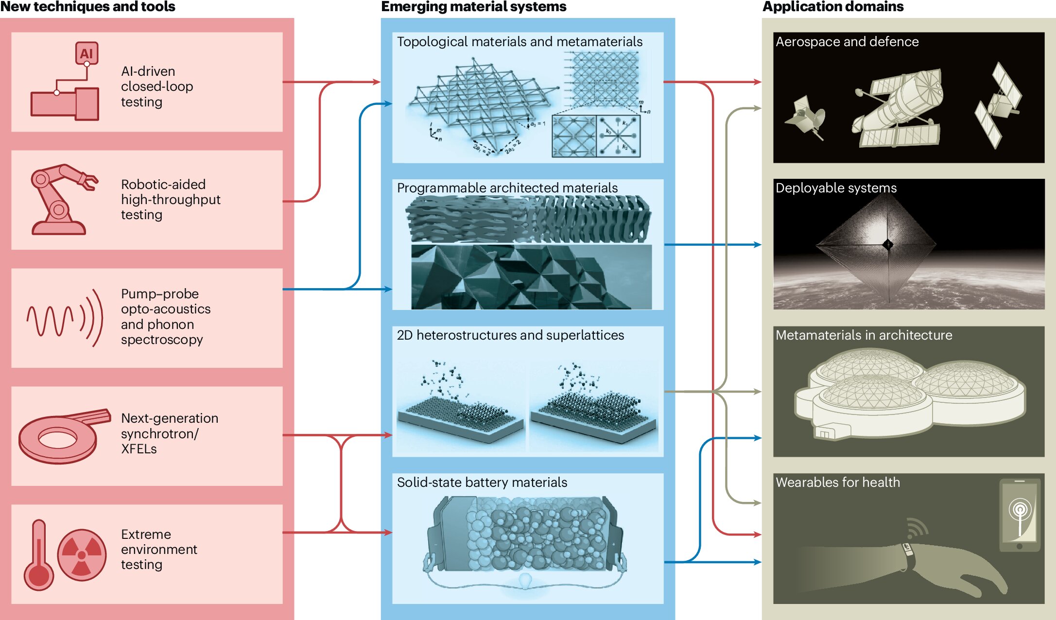
Researchers are gaining more precise ways to examine and test nanomaterials, a step that could improve products ranging from electronics to medical materials. University of Cincinnati assistant professor Hanxun Jin outlined the advances in a paper published in Nature Materials.
Jin, who works in UC’s College of Engineering and Applied Science, focused on tools that can measure and manipulate materials at extremely small scales. According to the university, those materials are used or studied for manufacturing, aerospace, medicine, energy storage and other fields.
Sharper instruments for smaller structures
Nanomaterials can behave in ways that larger materials do not, Jin said. Quantum dots used in television displays, for example, are semiconductor nanocrystals so small that researchers classify them as zero-dimensional, according to UC.
Jin said many nanomaterials are important in electronics and batteries, while others may be useful in water filtration systems designed to trap tiny heavy-metal particles. The difficulty, he said, is building instruments that can test such materials in useful ways.
Although some nanomaterials can have tensile strength greater than steel, Jin said they can also be fragile. He compared them to people because they contain defects, adding that those flaws are part of what makes them scientifically useful to study.
The paper points to progress in electron microscopy, X-ray imaging and acoustic methods. Jin highlighted hybrid photon-counting detectors, which UC said can produce highly clear X-ray images without background noise.
Jin also cited third-generation synchrotrons, which are operating in about 60 laboratories worldwide, according to UC. Those facilities generate very bright X-ray light, giving researchers a powerful way to study materials at tiny scales.
AI and automation speed testing
Artificial intelligence is also changing nanomaterials research, Jin said, by helping scientists gather larger datasets and interpret them more quickly. UC said robotics and computer modeling are making some experiments more automated.
Jin said those advances could open new engineering possibilities, including more ambitious nanoarchitectures. He told UC that such designs might one day contribute to concepts as far-reaching as a space elevator.
At Jin’s NanoBioMech Lab, researchers develop tools for designing biological materials at the nanoscale, according to UC. The work includes personalized health care and engineering applications, including bioprinting tissue and, in the longer term, possible transplant organs.
Doctoral student Elif Dursun said the field will need more complex and practical technologies. She pointed to printed body parts and skin tissue as examples of research directions that excite the lab.
UC said the researchers use scanning electron microscopy to examine materials such as collagen in human skin. Specialized software then creates 3D simulations showing how networks of collagen nanofibers stretch or shear when force is applied.
Jin said the goal is to understand the mechanical behavior of nanofibers well enough to design structures that resist breaking, or fail only when researchers want them to. He said different types of skin have fibers with distinct architectures and material properties, and that better design could improve toughness.
The paper, “In situ mechanical characterization of functional and architected materials,” was published in Nature Materials. The listed DOI is 10.1038/s41563-026-02601-x.
This story draws on original reporting from Phys.org.