
Cracking-assisted quantum dot printing produces 600-nm display pixels
A Nature Electronics team used controlled cracks to transfer quantum-dot pixels, demonstrating 600-nm emitters and a 341-ppi full-color panel.
By Priya Raghavan · Science Reporter
3 min read
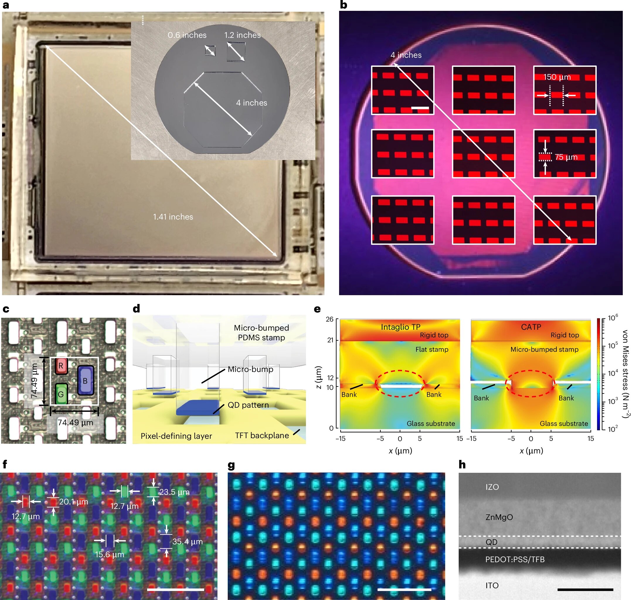
Researchers have reported a cracking-assisted quantum dot printing method that uses deliberately formed cracks to arrange light-emitting material into very small display pixels. The approach could help address a key manufacturing challenge for high-resolution quantum-dot LED screens: placing red, green and blue pixels precisely on an electronic backplane without mixing their colors.
The work, by researchers at the University of Cambridge and other institutions, was published in Nature Electronics, according to Phys.org. The paper describes laboratory demonstrations rather than a commercial display product.
How does cracking-assisted quantum dot printing work?
Quantum dots are semiconductor nanocrystals that can emit light. In the reported process, the researchers first deposit inorganic colloidal quantum dots as a thin film. The particles stick together through cohesive bonds, Phys.org reported.
The team then creates controlled cracks in that film. According to the Nature Electronics paper, breaking those bonds produces the intended pattern, allowing the patterned material to be picked up and transferred with precision onto a thin-film-transistor backplane, the electronic layer that controls display pixels.
That transfer step is aimed at making dense arrays of quantum-dot light-emitting diodes, or QD-LEDs. The paper says such devices are being studied for displays because of their color control and electrical stability, while large, high-resolution panels require uniform pixel placement across an active-matrix backplane.
What did the researchers demonstrate?
The smallest electroluminescent pixels reported in the paper measured 600 nanometers, and the team reported uniform pixelization over areas up to 4 inches. Those figures describe different aspects of the result: 600 nm is the minimum demonstrated emitting pixel size, while 4 inches is the reported area over which pixelization was uniform.
The researchers also made a cadmium-free, full-color active-matrix display with a resolution of 341 pixels per inch, the Nature Electronics paper says. Separately, they demonstrated a blue active-matrix display on a flexible form factor. The full-color result and flexible blue result should not be treated as the same prototype.
The authors wrote that the process can improve maximum luminance and operating lifetime compared with other quantum-dot patterning methods, which they attributed to control of interfaces at the nanoscale and a high packing density of quantum dots. The paper excerpt does not provide a quantified gain in either measure.
What the result does and does not show
QD-LEDs are of interest for augmented- and virtual-reality displays because high resolution and a wide color range are useful in those applications, according to Nature Electronics. The new technique offers a possible route for producing the required fine pixel patterns.
But the available research does not establish manufacturing yield, production cost, mass-production readiness, consumer-device adoption or a timetable for commercialization. Phys.org characterized the demonstrations as an indication of potential for scalable manufacturing, leaving those practical questions open.
This story draws on original reporting from Phys.org.