
Thin film substrates may play active role in future 3D chips
UC San Diego-led researchers found substrates can respond to working thin films, a result that could aid denser brain-inspired chips.
By Priya Raghavan · Science Reporter
3 min read
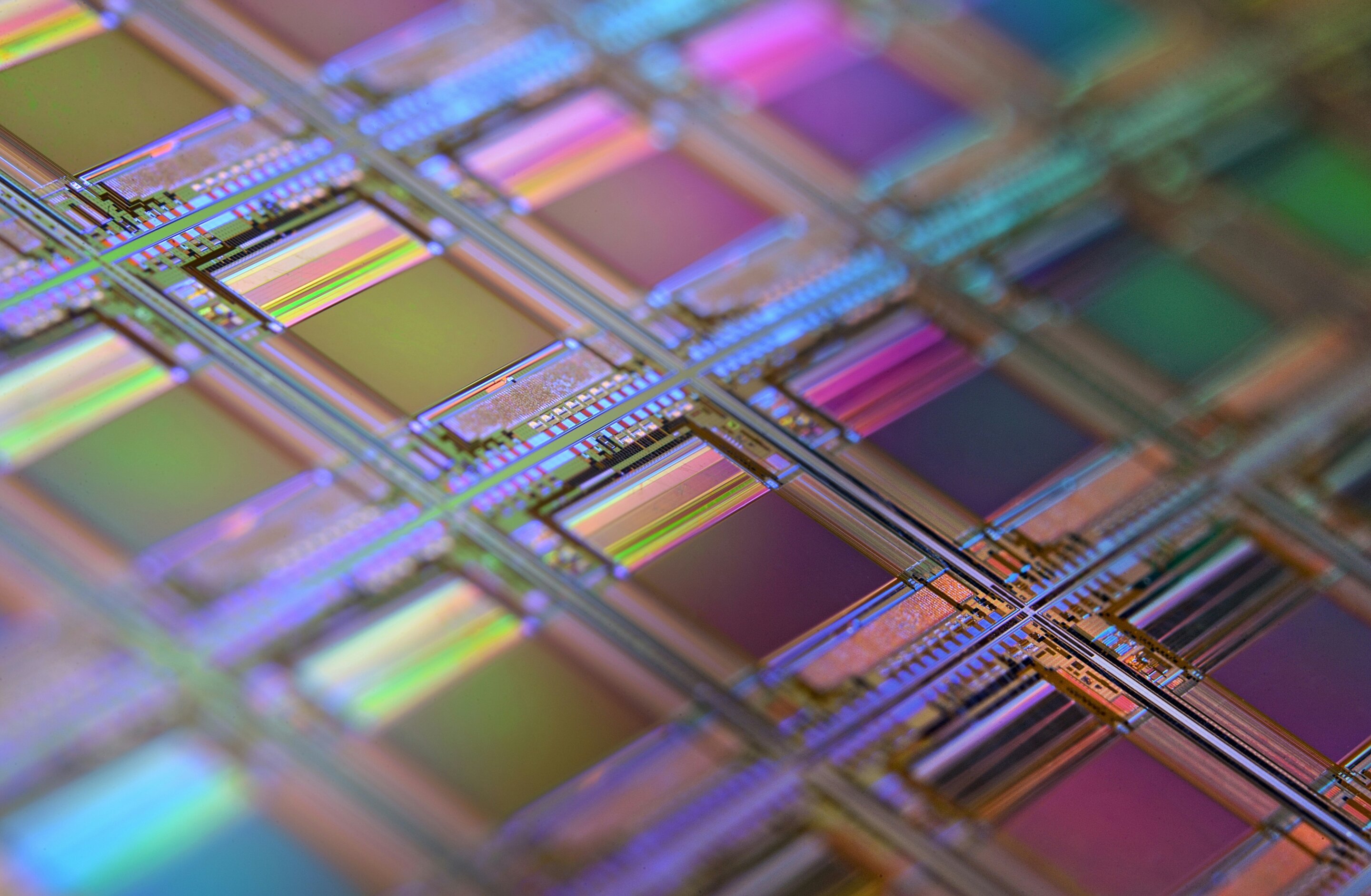
Thin film substrates may be more active than physicists and materials scientists have long assumed, according to a UC San Diego-led study published in Science. The finding matters because substrate behavior could give engineers another way to design dense three-dimensional chips for energy-efficient, brain-inspired computing.
UC San Diego said researchers observed changes in both a vanadium dioxide thin film device and the much thicker substrate beneath it when voltage was applied. That result challenges the common view that the substrate mainly serves as a passive support for the electrically active film.
The work came from the lab of Alex Frañó, an associate professor of physics at UC San Diego and a principal investigator and assistant director at the Quantum Materials for Energy-Efficient Neuromorphic Computing center. Q-MEEN-C, a U.S. Department of Energy Energy Frontier Research Center, studies quantum materials for neuromorphic computing, a field that seeks hardware inspired by the way brains process information.
What did researchers find in thin film substrates?
The team found that an operating thin film can imprint dynamic strain into its substrate, meaning the two parts exchange mechanical energy rather than behaving independently, according to UC San Diego. In plain terms, the support layer can move in response to the active film, and the film can also feel the substrate’s response.
The devices studied used vanadium dioxide thin films. UC San Diego said that when voltage is applied, an electric filament forms in the film and drives electrical spiking, a behavior researchers compare to signaling in neurons.
The observation was made with dark-field X-ray microscopy, a technique developed by graduate student Elliot Kisiel, now a Mayer Postdoctoral Fellow at Argonne National Laboratory. UC San Diego said the method lets researchers image a full device at once while also examining nearby areas with high fidelity.
The team initially looked at the substrate because X-ray lenses can absorb much of the X-ray signal, and the substrate offered a stronger signal for early tests. Instead of showing no response, the substrate changed along with the film.
How could this help 3D chips?
Current thin-film devices are generally connected in two dimensions, according to UC San Diego. Frañó’s team suggests that if a substrate can couple materials on opposite sides, researchers may be able to build devices on both sides of the same support, enabling more three-dimensional connections.
That approach could support chips that are denser and more interconnected, which is a key goal for neuromorphic computing. Such systems aim to perform tasks that people do with little effort, such as recognizing faces or distinguishing animals, using less energy than conventional computing requires.
UC San Diego said the team spent four years testing whether the substrate response was real. Researchers repeated the original experiment, changed parts of the sample such as substrate thickness and material, and used additional instruments.
Much of the verification work took place at Argonne National Laboratory, which operates a synchrotron that produces high-brilliance X-rays, and at Brookhaven National Laboratory, which UC San Diego described as home to the world’s only all-electric ultrafast electron microscope. That instrument can capture how a working device behaves under realistic operating conditions.
The Science paper, titled “Dynamic asymmetric strain imprinted into substrates by an oxide thin film,” lists Kisiel, Erbin Qiu, Wei He, Rourav Basak, Junjie Li, Ivan K. Schuller and Frañó among UC San Diego authors. UC San Diego said it follows a related ACS Nano paper from last year that used dark-field X-ray microscopy to study the thin film itself.
This story draws on original reporting from Phys.org.