
Stacked transistor design targets sub-1 nm chip performance
IBM says its nanostack architecture could nearly double transistor density and improve AI chip speed or efficiency without shrinking features below 1 nanometer.
By Maya Lindqvist · Senior Technology Correspondent
3 min read
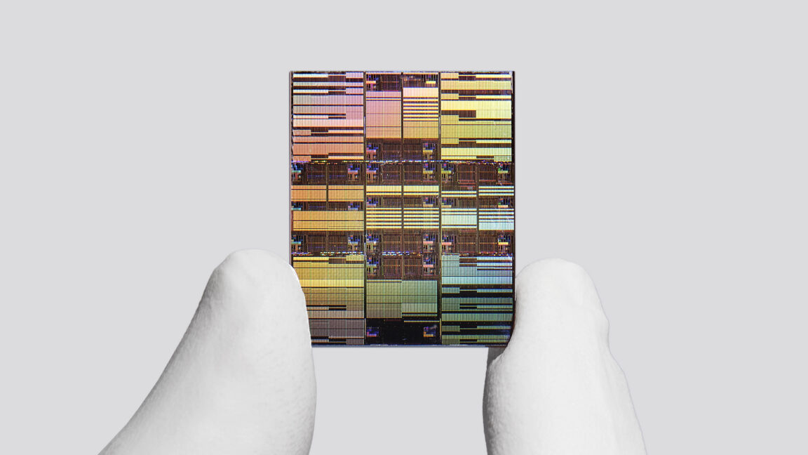
IBM says it has developed a chip architecture that can fit close to 100 billion transistors onto an area about the size of a fingernail, a density the company says is nearly double that of its prior chip technology. The company is presenting the design as a path to faster and more efficient chips for AI data centers.
IBM describes the technology as its first sub-1 nanometer chip platform, tied to what it calls a 0.7-nanometer, or 7 angstrom, node. That naming does not mean the chip uses physical features smaller than 1 nanometer; IBM says the label refers to performance gains associated with that class of scaling.
Chip node names have drifted away from literal feature sizes over several decades. IBM’s new claim centers on a structure called nanostack, which places transistors vertically in a staggered arrangement to pack more of them into the same surface area.
Jay Gambetta, director of IBM Research and an IBM Fellow, said in a media briefing that the design points toward more powerful computing without a matching rise in energy use. IBM says that balance is aimed at AI workloads, where data centers face pressure to increase compute capacity while controlling power consumption.
How the nanostack works
IBM says the nanostack approach builds on its earlier nanosheet transistor work, which underpinned the company’s 2-nanometer chip node announced in 2021. In the new design, the basic unit combines two transistors stacked and bonded together.
Each of those transistors contains three nanosheets, according to IBM. The company says each nanosheet is 5 nanometers thick, or about 15 rows of silicon atoms, with roughly 9 nanometers between individual sheets.
IBM’s technical reports project that the architecture could deliver 50 percent higher computing performance or 70 percent better energy efficiency compared with the company’s 2-nanometer node. IBM introduced the nanostack transistor architecture at the 2025 IEEE Symposium on VLSI Technology and Circuits in Kyoto.
The company also reported a 40 percent scaling improvement for static random-access memory, or SRAM, at the VLSI 2026 symposium. SRAM is used for fast memory operations that IBM says are central to many AI applications, though it can consume substantial power.
IBM attributes that SRAM gain to a staggered-channel design for SRAM bit cells. The company says the layout cuts cell height by 40 percent, allowing more memory cells to fit in a given chip area.
Commercial chips remain years away
IBM conducts semiconductor research but does not manufacture commercial chips for consumer devices or AI data centers. The company has worked with Japan’s Rapidus on manufacturing 2-nanometer chips based on nanosheet technology, and with Samsung on related semiconductor technology.
Other chipmakers have also adopted nanosheet-based approaches. IBM’s Huiming Bu, vice president of IBM Semiconductors Global R&D and IBM Research, said leading foundries use nanosheet technology for most 3-nanometer chips and all 2-nanometer chips.
IBM did not identify partners that might commercialize the nanostack design. Bu said chips using sub-1 nanometer node technology could enter production as early as five years from now, and more likely within a decade.
This story draws on original reporting from Ars Technica.